

Nvidia CEO Jensen Huang said on the 8th that he had received cutting-edge memory samples from Samsung Electronics and SK Hynix.
Nvidia CEO Jensen Huang stated at an event hosted by TSMC on the 8th, "SK Hynix, Samsung Electronics, and Micron are all excellent memory manufacturers, and they have all significantly expanded their production capacity to support vidia." He added, "We have received cutting-edge memory samples from these three companies." Addressing concerns about potential memory supply shortages, CEO Huang stated, "Our business growth is very strong, and shortages are possible across various sectors." He also indicated that memory prices may rise, depending on the company's operational situation.
At the same event, Nvidia CEO Jensen Huang stated that market demand for Nvidia's latest artificial intelligence (AI) chip, Blackwell, is "very strong," and that "TSMC's wafer demand is also growing significantly." He also stated that Nvidia's Blackwell-related chips are used not only in graphics processing units (GPUs) but also in central processing units (CPUs), network equipment, and switches (high-speed network equipment).
Meanwhile, TSMC CEO C.C. Wei stated, "Nvidia CEO Jensen Huang has made a wafer request, but the specific quantity is a trade secret." CEO Huang stated, "TSMC has provided excellent support in terms of wafer supply." He added, "Without TSMC, Nvidia could not have achieved what it has today." This is CEO Huang's fourth official visit to Taiwan this year.
At the event, Wei also referred to Nvidia CEO Jensen Huang as "a person with a market capitalization of $5 trillion." Nvidia became the first company to surpass a $5 trillion market capitalization last month.
In response, SK Hynix stated, "Our capacity for next year is fully sold out. We plan to significantly increase investment to prepare for the semiconductor industry's supercycle." It has been reported that Samsung Electronics is in talks with Nvidia to supply it with next-generation high-bandwidth memory (HBM4).
Three heroes vie for supremacy HBM4
SK Hynix, Micron Technology, and Samsung Electronics are fiercely competing to dominate the HBM4 market, estimated to be worth $100 billion (141 trillion won).
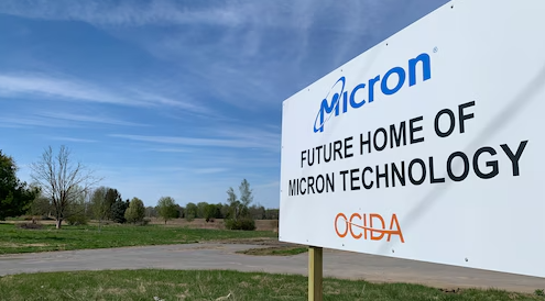
Following SK Hynix's completion of its next-generation HBM4 development and the establishment of its mass production system last month, Samsung Electronics has also begun preparations for HBM4 mass production. Meanwhile, US-based Micron recently announced that its next-generation HBM4 memory has begun shipping, claiming record-breaking performance and energy efficiency.
Micron CEO Sanjay Mehrotra stated, "The module has a bandwidth exceeding 2.8TB/s and pin speeds exceeding 11Gbps." These figures significantly exceed the JEDEC HBM4 official specifications of 2TB/s and 8Gbps.
Micron Technology has begun shipping 12-Hi HBM4 samples to support mass production on key customer platforms. The company claims that the product boasts industry-leading performance and best-in-class energy efficiency. Micron also stated that the key advantage of its 12-Hi HBM4 products lies in its proprietary 1-γ DRAM technology and innovative CMOS chip and packaging technologies.
HBM4E
Regarding HBM4E, which expands the basic design through custom options for the logic chip, Micron announced that it will offer not only standard products but also custom options for the basic logic chip.
CEO Sanjay Mehrotra stated, "Customization requires close collaboration with customers, and we expect HBM4E with a custom basic logic chip to offer higher gross margins than standard HBM4E." He added, "This technology, developed in collaboration with TSMC, enables major customers like NVIDIA and AMD to design custom accelerators with memory stacks optimized for low latency and better packet routing." Micron plans to gain a higher market share in the $100 billion HBM market this year than last year and expects revenue in the high-bandwidth memory segment to exceed $8 billion this year.
SK Hynix, a leader in the HBM field, announced that it delivered 12-Hi HBM4 samples to major customers, including NVIDIA, in March, ahead of Micron and Samsung, and began preparations for mass production in September.
SK Hynix's 12-Hi HBM4 samples use logic chips (the core component of the chip) manufactured using TSMC's 12nm process, and are claimed to have data processing speeds exceeding 2TB/s. However, it is not yet confirmed whether this product surpasses Micron's 12-Hi HBM4 product (bandwidth exceeding 2.8TB/s).
SK Hynix also plans to offer "custom HBM4E" products for its HBM4E product line to meet the needs of customers such as NVIDIA, Broadcom, and AMD.
The fourth generation HBM is coming soon
The Korea Advanced Institute of Science and Technology (KAIST) and its Terabyte Interconnect and Packaging Laboratory (Tera) research group outlined four more generations of high-bandwidth memory (HBM) in the middle of this year, boasting bandwidths up to 64 TBps and a stacking height of 24 layers—50% higher than HBM4.
The latest generation of HBM is HBM4, with bandwidth (data rate) up to 2 TBps, supporting up to 16 layers of Hi DRAM chip stacking, and a capacity of up to 64 GB. The HBM standard is published by JEDEC (Joint Electron Device Engineering Committee), with the first HBM standard (JESD235) released in 2013. Subsequent updates such as HBM2 (JESD235A), HBM2E, HBM3, and HBM3E have continuously improved bandwidth, capacity, and efficiency.

HBM3 and HBM4 employ forced air cooling (fins/fans) or forced water cooling (D2C – direct-to-chip) for heat dissipation. HBM5 will adopt immersion cooling in 2029, while HBM7 and HBM8 will use embedded cooling, integrating the heat dissipation mechanism directly into or near the chip.
HBM4 and HBM5 will use micro-bump (MR-MUF) chip stacking technology, while HBM6 through HBM8 will use bumpless Cu-Cu (copper-to-copper) direct bonding technology due to its high density, high performance, and improved signal integrity.
NVIDIA's Feynman (F400) accelerator will use HBM5 memory, with the entire GPU containing 400 to 500 GB of HBM5 memory. It is expected to release in 2028/2029.
The HBM6, launching in 2032, will employ an active/hybrid (silicon + glass) interposer, increasing its maximum stacked layer count from 16 for HBM5 to 20. This will allow for a capacity of 96 to 120 GB per stack.
The HBM7, launching in 2035, will offer a stacked capacity of 160 to 192 GB, with a maximum stacked height of 24 layers and a bandwidth of 24 TB/s, three times that of HBM6. The HBM8, launching in 2038, will see its bandwidth increased to 64 TB/s, with the same maximum stacked height of 24 layers. Its stacked capacity will also increase to 200 to 240 GB.
The HBM8 can utilize a double-sided interposer, with one side being HBM and the other side being HBM, LPDDR memory, or HBF (High Bandwidth Flash) memory. HBF memory combines the high bandwidth of HBM with the high capacity of 3D NAND. The HBM chip has a capacity of 240 GB; the LPDDR chip has a capacity of 480 GB; and the HBF chip has a capacity of 1024 GB.

Features of HBM4-8
We have summarized the known information in the table below, which lists the characteristics of HBM4-8:

This is a roadmap, and the further into the future, the less certain it becomes. We need to wait for JEDEC to release the official specifications for the next generation of HBM before we can trust the details within.
Source: Content compiled from chosun