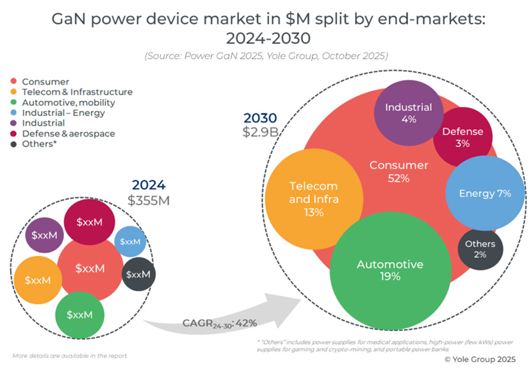
2025 marks a major acceleration in the development of artificial intelligence, coinciding with growing demand for efficient power supplies for data centers and telecom infrastructure. NVIDIA, in collaboration with companies like Texas Instruments, Innoscience, Navitas, and Infineon, is driving the adoption of GaN in 800V HVDC transmission systems, a market expected to capture 13% of the data center and telecom market by 2030.
The power GaN market grew more than tenfold from 2020 to 2025 and is projected to reach $2.9 billion by 2030, with a 24-30 year compound annual growth rate of 42%. Consumer applications are the primary growth driver, particularly fast chargers up to 300W, as well as new opportunities such as overvoltage protection (OVP) and home appliances. By 2030, the consumer and mobile sectors will account for over 50% of the market share.
Despite delays in the adoption of xEV powertrains, automotive and mobility remain another major growth driver. GaN has been used in lidar systems for ADAS and is expected to achieve scale in on-board chargers (<11kW), DC-DC converters, audio, and high-end electric vehicles. By 2030, this sector will account for approximately 19% of the market share.
Industrial and power grid applications are emerging as the third largest growth driver for power GaN. In the energy sector, GaN is booming in photovoltaics and battery energy storage systems (BESS)/portable storage, with Enphase launching its first GaN-based microinverter. In the industrial sector, robotics and motor drives are expected to present strong opportunities, with their adoption expected to accelerate around 2028-2029. By 2030, these sectors will collectively account for approximately 11% of the total market.

IDMs and foundries reshape the power GaN ecosystem
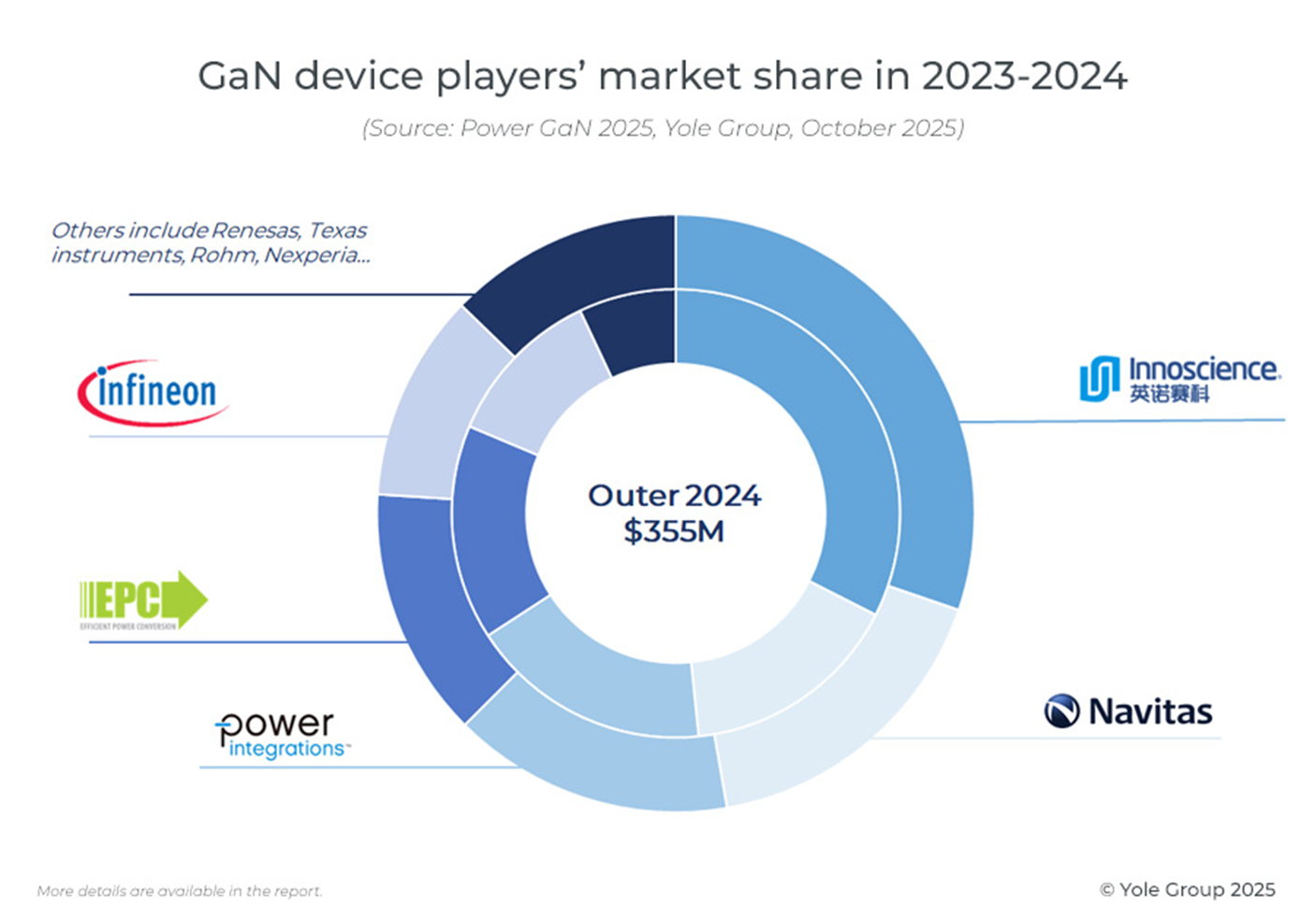
Since 2023, the power GaN industry has entered a period of consolidation, driven primarily by major mergers and acquisitions, such as Infineon's $830 million acquisition of GaN Systems and Renesas Electronics' $339 million acquisition of Transphorm. Over the past few years, over $1.25 billion has been invested in the sector, with startups like Wise Integration raising $16.4 million, highlighting strong market momentum. Other players are also accelerating their efforts: STMicroelectronics is building an 8-inch GaN wafer fab, Nexperia is expanding its e-mode platform, and Rohm has launched EcoGaN devices. Meanwhile, Samsung is preparing to release GaN products in 2026. As for ON Semiconductor, while the company has remained relatively quiet, its 2024 GaN technology paper and strong position in silicon and silicon carbide make its entry into the GaN market a must.
However, challenges remain. The ongoing intellectual property dispute between EPC, Infineon, and Innoscience could slow GaN's adoption. Despite TSMC's exit, foundries continue to play a crucial role, with X-Fab, GlobalFoundries, and new entrants such as Powerchip and Polar Semi all expanding their production capacity. Collaboration between epitaxy fabs (such as IQE and X-fab) and IDMs (integrated design manufacturers) has enhanced supply resilience. The power GaN market landscape is evolving, shaped by consolidation, an IDM-led model, and strategic foundry-epitaxy fab alliances.

Device innovation combined with wafer scaling will drive the next wave of cost reductions
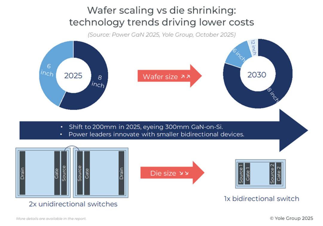
While 6-inch GaN-on-Si still dominates, the industry is rapidly transitioning to 8-inch wafers, which are expected to meet over 80% of demand by 2030. Regarding 12-inch wafers, Intel demonstrated initial results for 12-inch GaN on TRSOI in the fourth quarter of 2024, concurrently with Infineon's demonstration of 12-inch GaN-on-Si. Infineon announced sample availability in the fourth quarter of 2025, but does not anticipate high-volume production within the current forecast period.
GaN epitaxy is the most expensive step in HEMT production and is a key focus for optimization. Aixtron's G10 MOCVD platform is expected to reduce epitaxy costs, while VIS achieved high-volume production of 8-inch GaN on QST in 2024, utilizing Qromis substrates to increase yield and reduce costs. Furthermore, IMEC's recently launched 300mm GaN project (based on silicon and QST substrates) is expected to further reduce GaN device manufacturing costs. At the device level, progress includes 1200V+ GaN (on sapphire and QST substrates) and 600-650V bidirectional devices, both expected to be launched by Navitas and Infineon in 2025. These devices are already being used by Enphase in its next-generation microinverters, saving BOM costs by replacing two back-to-back switches. However, GaN integration is not plug-and-play: EMI management and system-level design adjustments remain critical for its application.

Source: Content compiled from Yole
Reference Link
https://www.yolegroup.com/product/report/power-gan-2025/?utm_source=PR&utm_medium=email&utm_campaign=PR_Power-Gan-Market_Oct2025


