Imagine trying to carve a tiny, intricate sculpture into a block the size of a fingernail, over and over again, billions of times, with little room for error.
This is exactly what chipmakers do when they etch intricate patterns into silicon wafers to create the semiconductors that power most of the electronic devices and technology around us. The need to carve these patterns with extreme precision becomes increasingly urgent and challenging as we demand more power and speed from smaller devices.
To meet the growing precision standards of semiconductor production, a research team recently introduced a breakthrough technology called DirectDrive that brings unprecedented precision to the plasma etching process used to make computer chips. The innovation is expected to support the development of next-generation electronics, especially those used in artificial intelligence systems that require highly compact and ultra-high-speed circuits.
From kitchen to laboratory
DirectDrive wasn't the product of a week or a month of research. It took 20 years to come together. Back in 2006, Patrick Pribyl, an engineer at the University of California, Los Angeles (UCLA), came up with an idea for better control of plasma during the etching process used to make chips.
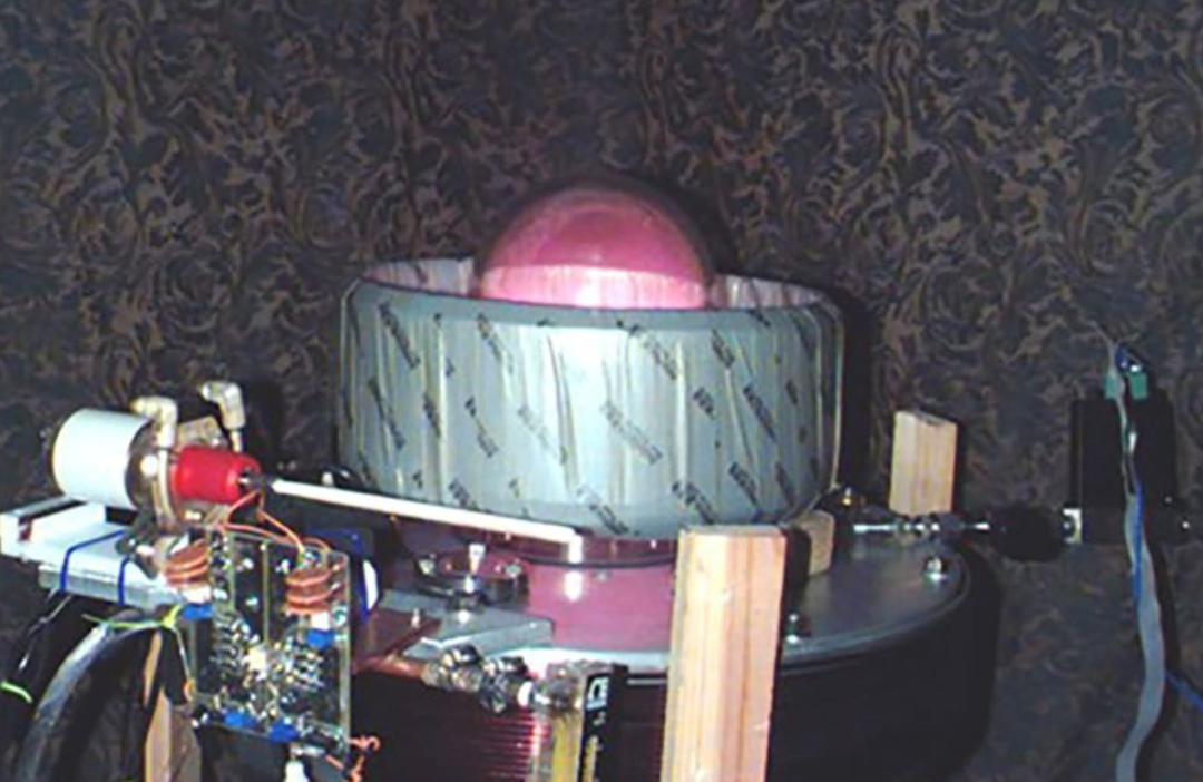
Pribyl designed a device that could quickly switch the radio frequency (RF) energy that drives the plasma, allowing for finer etching control. To test his idea, he built an early version of an RF switching system in his kitchen, which was crude but worked.
However, despite the promise of this approach, companies weren't ready to adopt it yet. The science behind it wasn't mature yet, and turning kitchen experiments into reliable industrial technology would take years of hard work. But Pribyl wasn't about to give up. He teamed up with another UCLA physicist, Walter Gekelman.
Together, the two raised money and arranged for enough equipment to continue working on the RF switching system. Meanwhile, several other scientists joined the decade-long research.

The original kitchen prototype
In 2015, they jointly received a grant from the National Science Foundation (NSF) under the Global Plasma Laser Imaging (GOALI) program to conduct this research.
Pribyl and his team spent the next decade working with lasers and custom devices. They measured the behavior of ions under the plasma pulses and noticed changes in various properties related to their movement and density. They used the same radio frequency energy used in devices such as Wi-Fi and cell phones, but at higher powers, to control the plasma.
"We realized early on that this was important to industry," Gekelman said, and they believe the new method could be a huge success once it reaches the market.
The limiting factor in making more advanced chips is the minimum size at which nanoscale electronic components can be reliably etched to work properly. Faster, more powerful chips require smaller and more complex structures.
The key to Pribyl's method is a simplified process of rapidly switching (or "pulsing") radio frequency electricity to create and drive plasma inside a semiconductor etcher. At relatively low power, radio frequency energy (commonly called "RF" energy) can wirelessly transmit data such as text messages and streaming movies. At higher powers, it can create charged matter, known as plasma. RF energy is typically used to partially ionize a chemical mixture inside an etcher, causing it to transition from a gaseous state to a plasma. The charged particles in the plasma then rain down on the silicon wafer, eating away at carefully designed, unmasked areas of the chip, leaving behind intricate and tiny circuits.
To understand the role of RF energy switching in semiconductor etching, imagine a sculptor switching between chisels of different shapes and sizes as he carves a block of marble. The sculptor might use one chisel to chip away at a large block of marble, then switch to another to carve out delicate details. Similarly, the RF energy used to create the plasma inside the etcher must be stopped, started, and switched periodically to control the power of the plasma and the depth of etching.
Unlike a sculptor who simply stops hammering when he wants to switch tools, the plasma continues to "chisel" the silicon for several seconds while the RF energy mechanically switches to different power levels. However, fast-switching methods can turn the power on or off in 50 microseconds-less than one-tenth the time required before.
Previously, switching between different power levels in a plasma process took too long, resulting in imprecise results. Pribyl's method, now called DirectDrive, can make these switches in just 50 microseconds, tens of thousands of times faster than before.
Specifically, DirectDrive technology rapidly pulses RF energy thousands of times per second, allowing for more precise control of the plasma to reliably etch smaller electronic components. In fact, their etch process improved significantly after adopting the pulsed plasma technique.
Their ultimate results were met with skepticism. "They said, 'This can't be possible,' " Pribyl recalls of the initial reaction of others in the industry. "It just blew the minds of the entire semiconductor community that this could actually be done."
From the lab to the factory floor
However, this breakthrough did not happen overnight. Like many scientific projects, it took years of painstaking experiments and precise measurements in the lab. "Essentially, what we did was design the experiment and make the measurements," Gokelman said.
Pribyl added: "We can do better than the factory floor."
Gokelman, Pribyl and others spent nearly 10 years in their UCLA lab, using lasers and custom detectors to observe the complex 3D motion of ions in pulsed plasmas, as well as properties such as density, temperature, electric and magnetic fields.
"We also measured how fast the ions were moving," Gekelman said, "whether they were moving straight down or slightly to the side, and whether the angle at which they hit the wafer was consistent across the wafer."
Their detailed measurements provided a more comprehensive understanding of the fundamental properties of plasmas and a rigorous scientific basis for scaling pulsed plasma processes to industrial levels. Gekelman and Pribyl's collaborators at the University of Michigan made further contributions, using computer modeling to simulate the behavior of plasmas in areas of the machine that could not be directly observed in the UCLA lab.
"In addition to the new insights into nature and the foundations for new technologies, these labs attract and train scientists and engineers who can use their ideas to advance American industry," said Slava Lukin, director of the National Science Foundation's plasma physics program. "Students from these labs are often hired by industry before they even start writing their doctoral dissertations."
The technology now surpasses existing technologies, enabling smaller, denser and 3D semiconductor devices to be etched with angstrom-level precision (for perspective, the width of a single hydrogen atom is about one angstrom). The latest plasma etching equipment based on this technology is used to quickly produce advanced circuits in the spotless clean rooms of chip manufacturing plants.
As the industry's first solid-state plasma source, the technology's plasma response speed is 100 times faster than previous plasma sources, thereby reducing EUV pattern defects. Thanks to this technology, it can support the miniaturization of all-around gate (GAA) transistors, 6F 2 DRAM and 3D NAND devices, and can be expanded to 4F 2 DRAM, complementary field-effect transistors and 3D DRAM. These devices require extremely challenging key etching steps and precise extreme ultraviolet (EUV) lithography patterns to form complex 3D structures. In order to create tiny features with higher aspect ratios, angstrom-level accuracy is required, which is beyond the capabilities of current mainstream plasma etching technology.
As one researcher said, every change in semiconductor technology is backed by years of development and years of scientific research.
Reference link: https://www.yahoo.com/news/20-years-research-directdrive-plasma-161302527.html?guccounter=1
Source: Semiconductor Industry Observation


