In 1965, Intel co-founder Gordon Moore proposed Moore's Law. For more than half a century, this law has driven improvements in integrated circuit (IC) performance and reductions in cost, becoming the foundation of modern digital technology. Moore's Law
states that the number of transistors on a semiconductor chip doubles approximately every two years.
For a long time, technological development followed this law. But things are starting to change. In recent years, shrinking chip circuit dimensions has become increasingly difficult, with line widths now down to a few nanometers (nm). Engineers face physical limits, increasingly complex manufacturing steps, and rising costs. Shrinking circuit dimensions also mean lower yields, making it more difficult to produce large numbers of usable chips. Furthermore, building and operating semiconductor foundries requires significant capital and expertise. Consequently, many believe that Moore's Law will no longer hold.
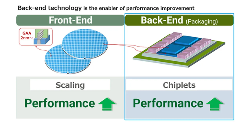
The end of Moore's Law has ushered in a new advancement: chiplets.
A Chiplet
A chiplet is a small portion of a chip (die) that performs a specific function. Originally, it was part of a single, larger chip. Through chiplet integration, multiple chiplets can be combined into a single package, creating a complete system.
In the past, all chip functions had to be built on a single wafer. This meant that if even one part of the chip had a defect, the entire chip had to be discarded. With chiplets, only good chips (known good die, or KGD) are used—significantly improving manufacturing yield and efficiency.
Heterogeneous integration is an integration process that allows different chips with different functions, manufactured using different processes, to be combined into a single chip package. Small chiplets are particularly effective for mixing and combining different types of circuits. For example, high-performance computing components can be manufactured using the latest semiconductor processes, while memory and analog components can be produced using more traditional, cost-effective technologies. This balance helps improve performance while maintaining low costs.
The automotive industry is particularly interested in this approach. Some major automakers have begun using this technology to develop system-on-chips (SoCs) for future vehicles, with plans to use them in mass-produced vehicles after 2030. A major advantage of chiplets is that they can help manufacturers improve the performance and functionality of automotive semiconductors, more efficiently enhance AI computing and graphics processing capabilities, and increase production volumes.
Some automotive components must meet stringent safety standards. These components, known as functional safety components, typically use older, more mature semiconductors. However, modern systems like advanced driver assistance systems (ADAS) and software-defined vehicles (SDVs) require more powerful chips. This is where chiplet technology comes in. Chiplet technology allows manufacturers to more quickly customize SoCs to each automaker's needs by combining microcomputers for functional safety components, large memory capacities, and powerful AI processors for autonomous driving.

The applications of chiplet
These advantages aren't limited to automotive applications. Chiplet technology is also expanding into other areas such as artificial intelligence and telecommunications, driving innovation across numerous industries. Chiplet technology is rapidly gaining popularity and becoming a key technology for the future of the semiconductor industry.
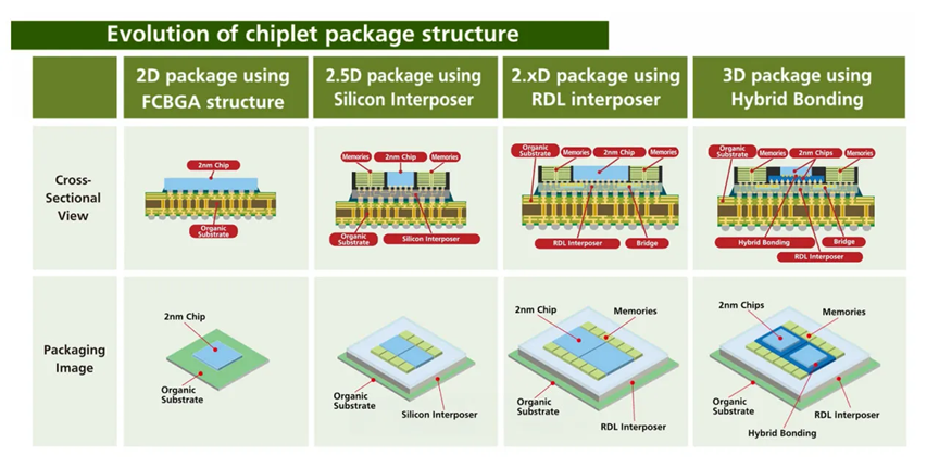
Chiplet integration relies on a technique for connecting multiple chips in a compact and high-speed manner. Interposers are a key component in achieving this goal. An interposer is an intermediate layer, typically made of silicon, that sits beneath a chip, connecting the chips like a circuit board and enabling communication between them. The better the interposer, the tighter the connections between the chips, and the faster they can exchange electrical signals.
Advanced chiplet integration technology also plays a key role in efficient power delivery. Adding numerous tiny metal connections between chips creates sufficient paths for current and data transmission, even in confined spaces. This not only enables high-speed data transmission but also makes full use of the limited space within the chip package.
Today, the mainstream approach to chip integration is 2.5D integration, which involves placing multiple chips into a single package. However, the next major advancement is 3D integration, which involves vertically stacking chips. In a 2.5D structure, chips are arranged side by side on an interposer to achieve high-density connections. In contrast, 3D integration uses a technology called through-silicon vias (TSVs) to stack chips vertically, enabling higher integration densities.

By combining flexible chip design (which separates different functions and circuit types) with 3D integration, engineers can build faster, smaller, and more energy-efficient semiconductors. Stacking memory and processing units directly together enables high-speed access to large amounts of data, which is highly beneficial for rapidly executing artificial intelligence and other high-performance processes.
On the other hand, vertically stacking chips also introduces new challenges. Heat accumulates more easily, making thermal management and maintaining high manufacturing yields more difficult. To overcome these issues, researchers around the world are developing new approaches to advanced packaging technology to better address thermal challenges. However, this has not slowed the pace of innovation. The combination of chiplets and 3D integration is now seen as a disruptive innovation, potentially replacing Moore's Law and ushering in the next era of semiconductor development.
Source: Content compiled from rapidus


