

SK Hynix has upgraded its factory in Wuxi, a key DRAM production base in China. This upgrade is seen as a significant expansion of its production facilities, given that the company completed its process conversion amidst US sanctions on Chinese semiconductors.
The 1z process was upgraded
Industry insiders revealed on the 14th that SK Hynix has upgraded its existing 1z process to 1a process at its Wuxi plant. Currently, the Wuxi plant has a monthly DRAM production capacity of 180,000 to 190,000 wafers based on 12-inch wafers, with approximately 90% of that capacity handled by the 1a process. The company announced the Wuxi plant upgrade plan during its earnings call in January 2024, and the upgrade was completed in just two years.
Depending on the microfabrication process, DRAM is divided into different generations. 1z represents the third generation 10nm DRAM, while 1a represents the fourth generation. Higher generations generally indicate better performance. SK Hynix is now able to produce higher-performance DRAM at its Wuxi plant.
As the Wuxi plant is SK Hynix's core production base, its process upgrade has attracted significant attention. The Wuxi plant accounts for 30% to 40% of the company's total DRAM production.
If the process upgrade had not been completed due to US regulations on semiconductor equipment, it could have disrupted production and business operations. However, these concerns appear to have been alleviated.
Extreme ultraviolet (EUV) lithography
1a DRAM requires extreme ultraviolet (EUV) lithography technology. However, due to US export restrictions, EUV equipment cannot be imported into China.
As an alternative, SK Hynix adopted a method of completing the EUV process required for fine circuit implementation in South Korea and completing the remaining processes in Wuxi.
Despite the complexity of the process and high logistical costs, the transformation of the Wuxi plant into a 1a process production line is seen as crucial to SK Hynix. This is not only a key foundation for SK Hynix to meet the demands of the Chinese and global markets.
At the Q2 earnings conference last year, SK Hynix President Song Hyun-jong stated, "The Chinese factory is not only crucial to SK Hynix, but also to the global supply and demand of memory semiconductors. To ensure its continued operation, we will closely monitor US regulatory developments and maintain close communication with governments around the world."
Since commencing production in 2006, SK Hynix has invested trillions of won in the Wuxi plant.
Meanwhile, SK Hynix expects to accelerate the upgrade of its domestic DRAM wafer fabs to the equivalent of sixth-generation 1c process technology. Investment in the 1c upgrade will be concentrated in the M14 and M16 wafer fabs located in Icheon. The future production structure will be: general-purpose DRAM products will be manufactured in China, while advanced DRAM products will be manufactured in South Korea.
SK Hynix accelerates production expansion
An SK Hynix executive said the company plans to bring forward the opening of one new factory by three months and begin operations of another new factory in February due to surging memory demand putting pressure on global supply.
This decision by the South Korean chipmaker comes as a global shortage of memory chips drives up prices for consumer electronics such as smartphones and PCs and slows the construction of data centers needed for artificial intelligence.
"We must support the memory consumption of artificial intelligence infrastructure," said Sung-Soo Ryu, CEO of SK Hynix America, in an interview with Reuters.
Ryu stated that his company is a key partner of Nvidia. The supplier will open its first factory at its new chip plant in Yongin, South Korea, three months ahead of schedule in February 2027. In addition, the company plans to begin deploying silicon wafers next month at its new M15X wafer fab in Cheongju, South Korea, to produce high-bandwidth memory (HBM) chips.
Reuters reported that this is the first time SK Hynix has decided to advance its production plans at its Yongin plant. Previously, a local media outlet, citing anonymous industry sources, reported on the company's HBM production plans.
Located in Yongin, 40 kilometers (25 miles) south of Seoul, this wafer fab is part of the company's planned 600 trillion won ($407 billion) "semiconductor cluster," which will eventually house four wafer fabs.
Mr. Ryu declined to disclose details of the production capacity of the first phase of the Yongin plant, but said the new capacity would be "very helpful" in meeting customer demand.
Analysts estimate that the current capacity of the first wafer fab in Yongin will be comparable to that of the company's multi-fab complex in Icheon.
Ryu said that customers, including those working on hyperscale data centers, are increasingly seeking multi-year supply agreements - a departure from the more common one-year contracts of the past - as they scramble to secure long-term supplies.
According to market tracker TrendForce, the global memory chip market is experiencing unprecedented growth, with prices for some products rising by more than 300% year-on-year in the fourth quarter alone, driven by surging demand for artificial intelligence infrastructure leading to tight capacity.
Ryu said that SK Hynix reviews its production plans monthly to ensure it can support its customers. Ryu stated, "There is a structural shift taking place (in the memory chip market)," adding that he has not yet seen any signs of a slowdown in demand.
He said, "We are seeing tremendous demand."
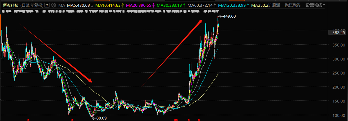
SK Hynix, the world's second-largest memory chip manufacturer after Samsung Electronics, has seen its stock price rise by 280% over the past year.
Source: Compiled from Reuters, etc.